Hello,
As you’ve probably seen (if you read my blog), my previous bus master was ugly, small and uncomfortable to use.
It was the high time to make something new… :)
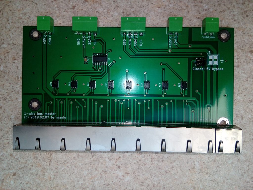
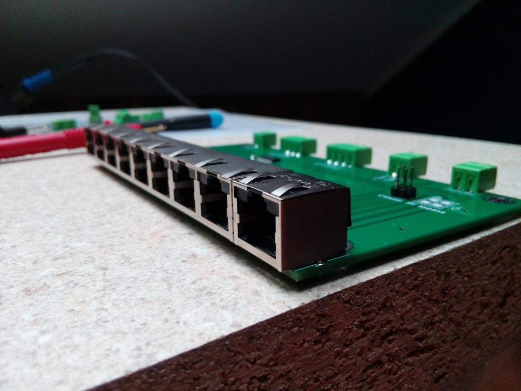
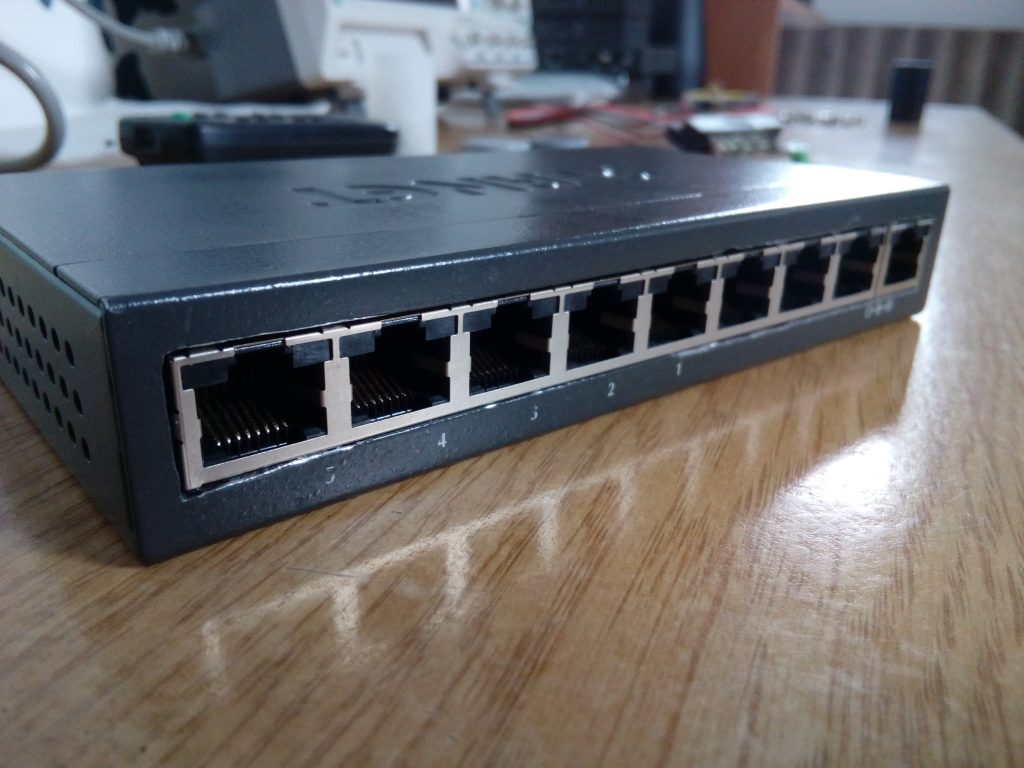
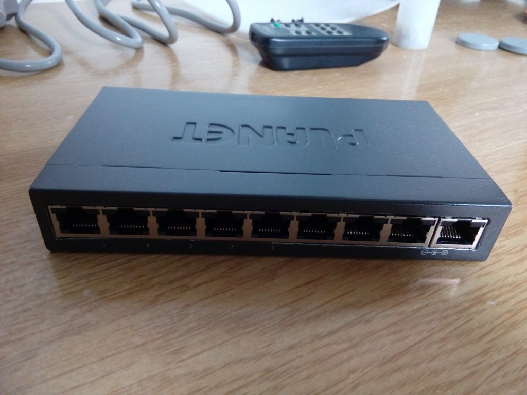
Connecting 1-wire buses should be as easy as connecting a LAN cable to the switch. As all my 1-wire buses are wired using the ethernet cables, so I decided to use the 8P8C ( wrongly referred as RJ-45) connectors.
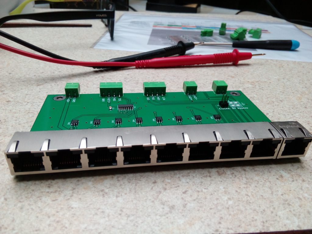
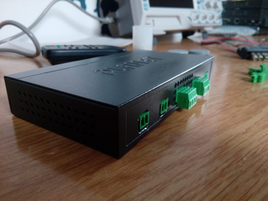
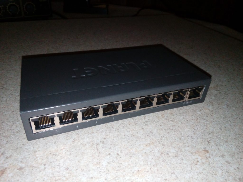
My plan was to take some old ethernet switch, remove its PCB and create my own to fit perfectly instead of the original one. After quick research I’ve decided to use the old Planet switch for this purpose ;)
It has a reliable, compact size metal case which I like very much.
I only had to modify it a little (using a Dremel) to suit my needs.
At the beginning I was planning to make the PCB myself with home thermal-transfer method, but over a designing time I’ve change my mind :)
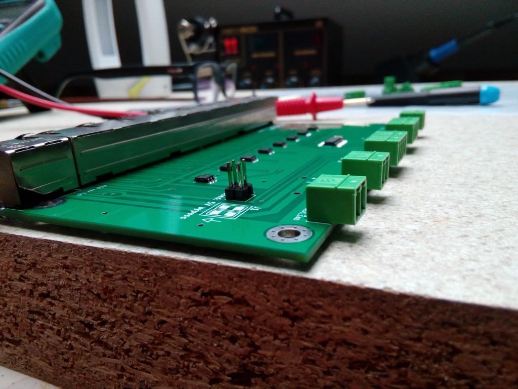
For the first time I decided to try a JLCPCB prototype manufacturer. It was a great decision! First of all because the quality of the boards cannot even be compared with a home-made PCBs, secondly because It would be really hard if not impossible (with reasonable size and look) to fit it all on one-sided PCB. The minimum at JLCPCB is a two layer board. Finally - the price was really great and acceptable - even including the shipping cost to the Europe!
Before you ask: this is not a sponsored article! :)
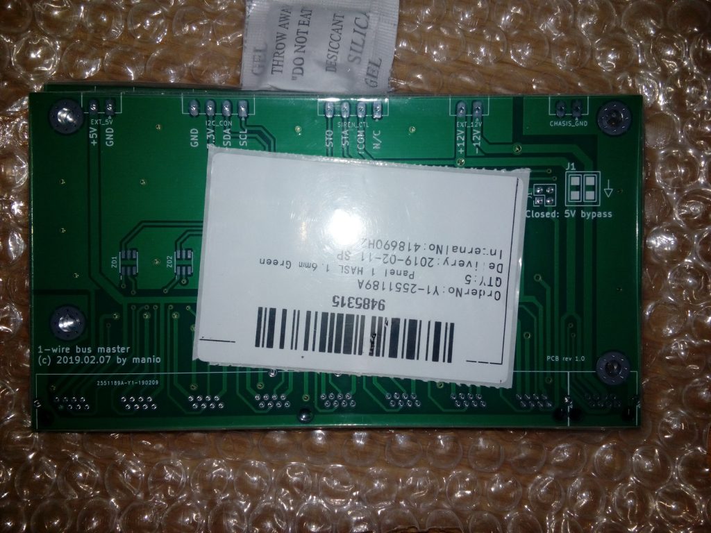
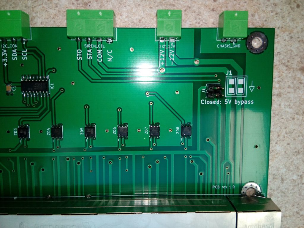
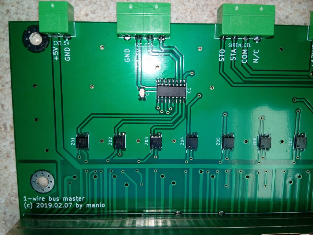
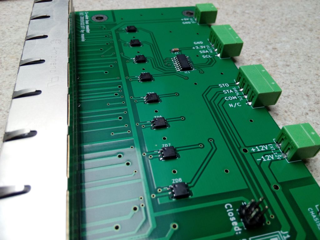
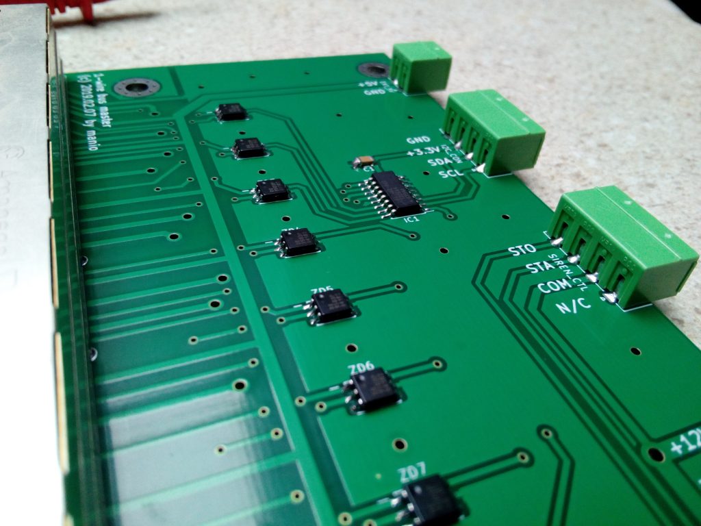
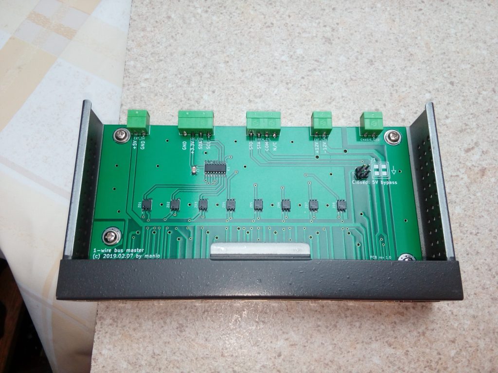
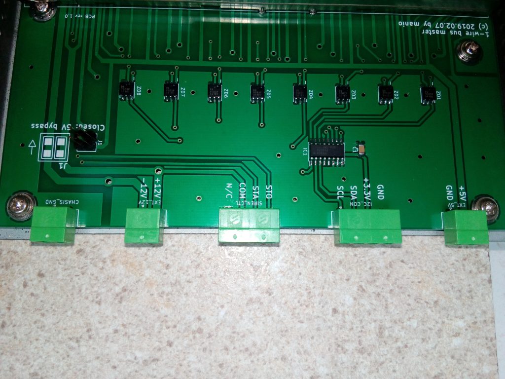
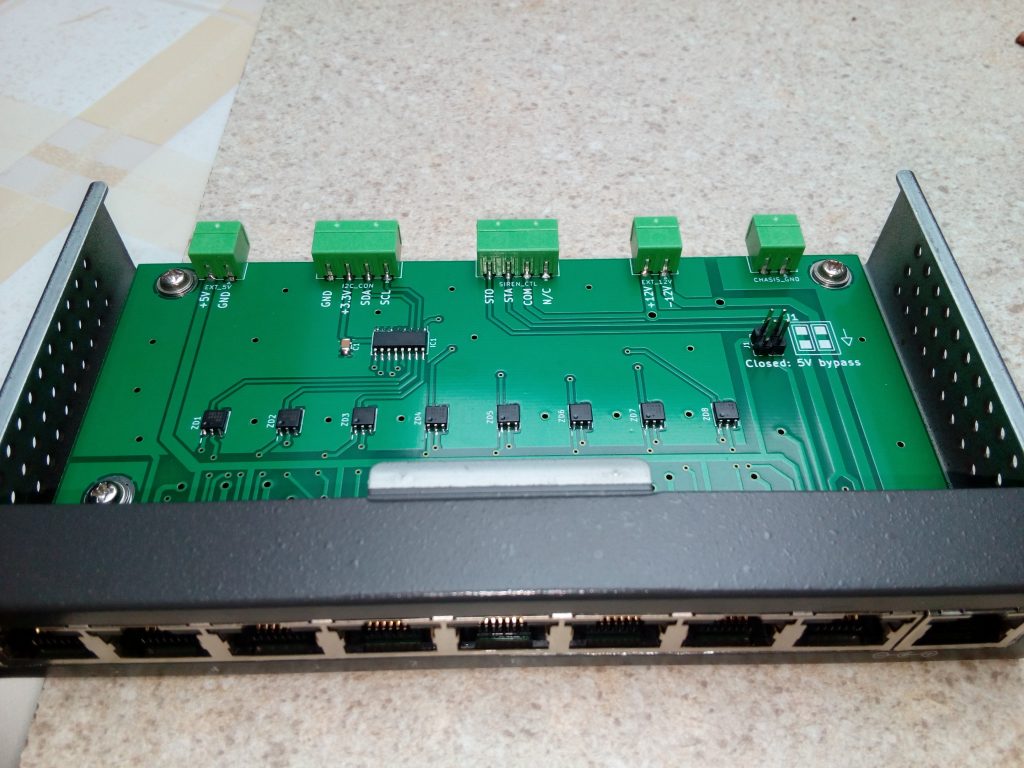
My bus connectors has to provide additional lines with voltages then only 1-wire bus data and ground. I needed to provide power for my PIR sensors and slave devices (I am not using a parasite power). As a result - I found and decided to use a 1WRJ45 standard for wires in 8P8C.
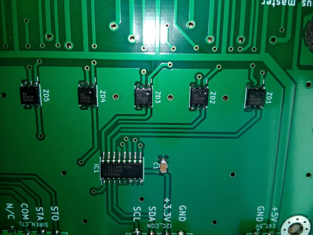
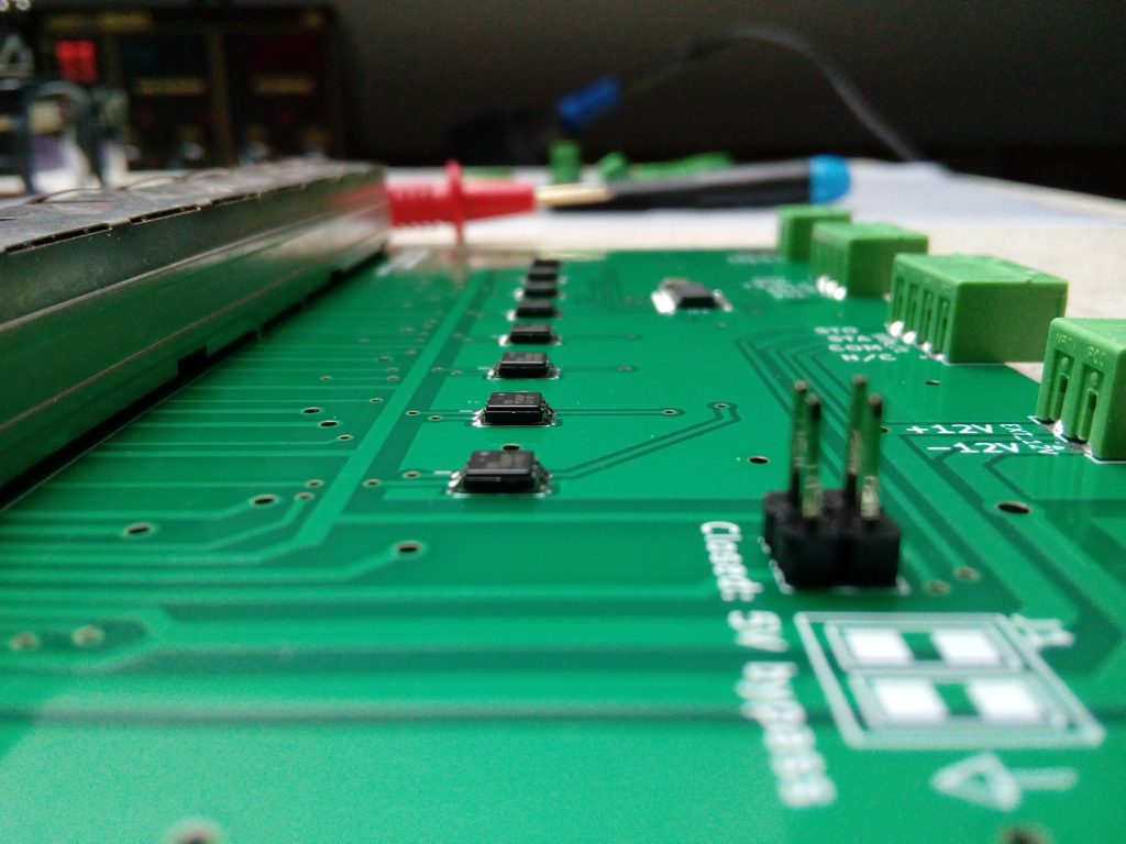
As an additional precaution I’ve also added a DS9503P ESD protection diodes to each channel of my DS2482-800 chip. I didn’t have this before.
Also for the first time I was using a KiCad EDA for designing the whole PCB. KiCad and its community is great! I also contributed a new footprint for the RJHSE5380-08 Amphenol connector because it was missing in the library.
It should be now available for everyone using KiCad :)
I had a problem with following the tutorials on the official JLCPCB pages regarding the export settings. The settings which are provided on the images are in conflict with the video tutorial linking on the same page. Examples? Look:
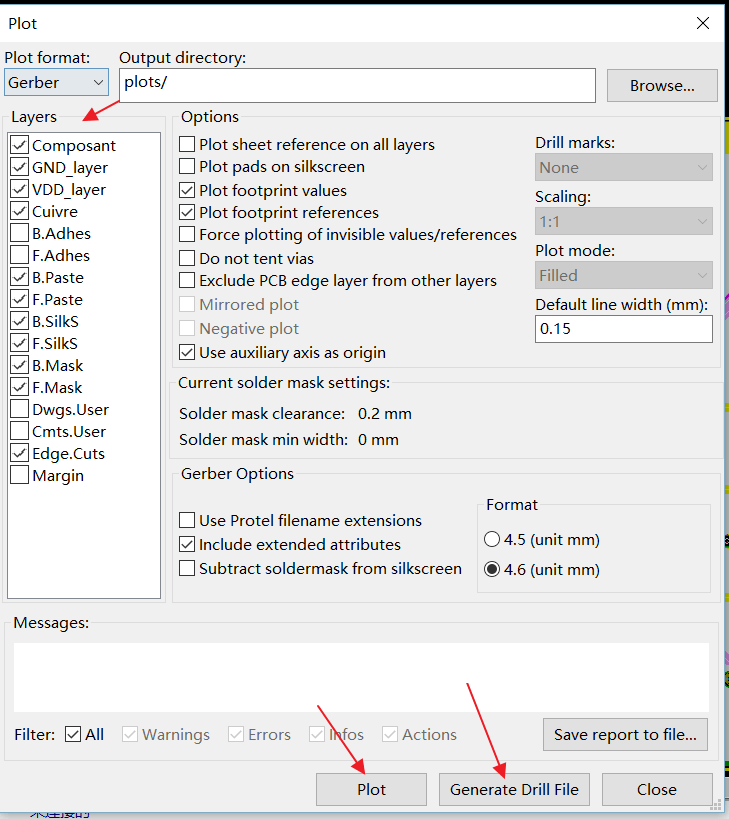
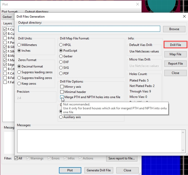
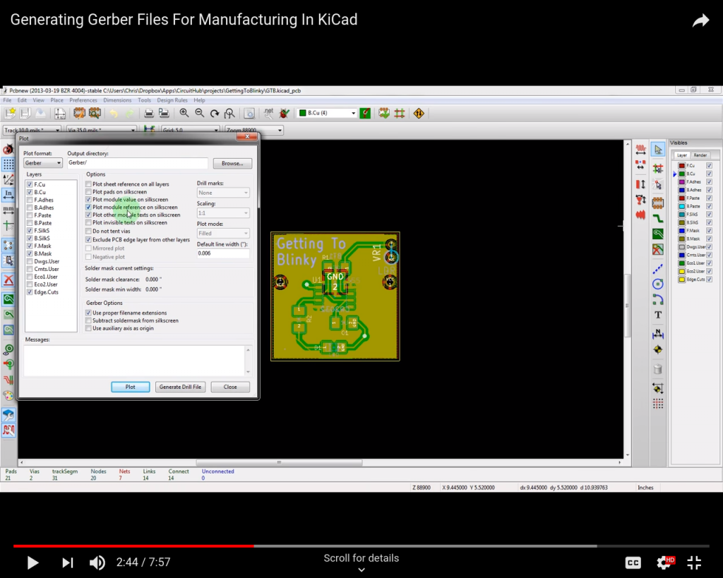
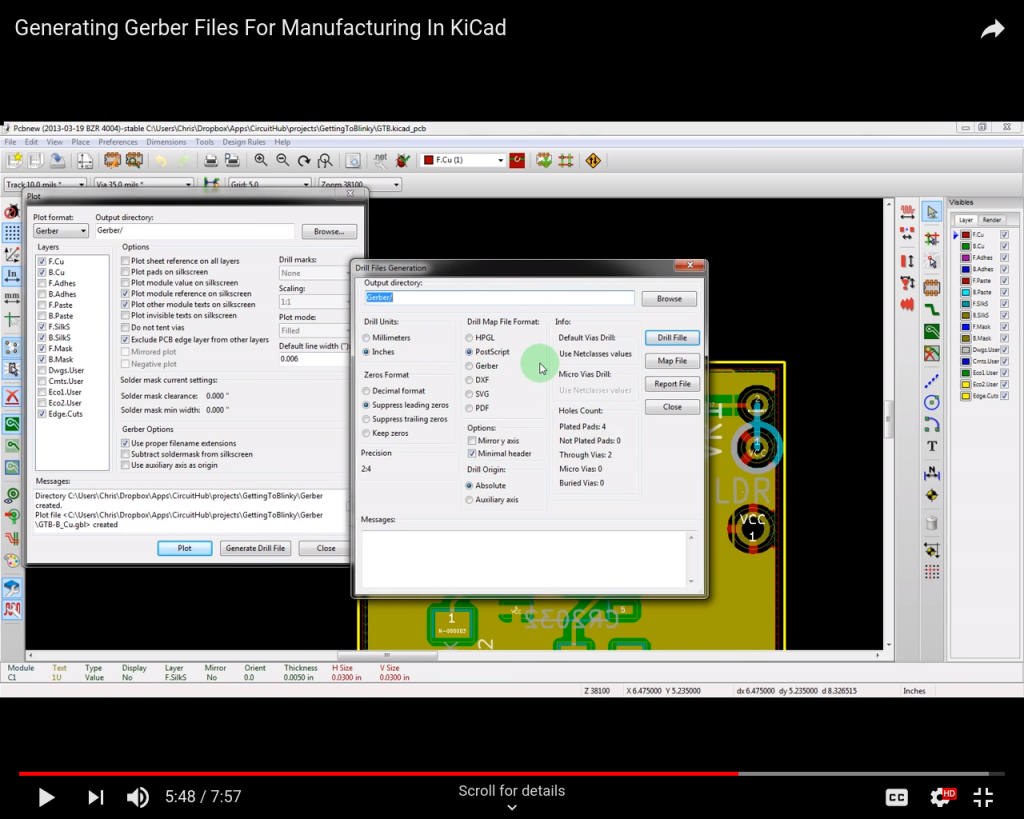
As a result I just decided to leave the settings as default and only removed the unnecessary layers. For the reference, I’ve set it like this:
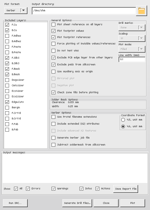
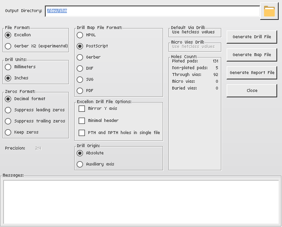
Fortunately I have no issues with the manufactured board with the above settings! :)
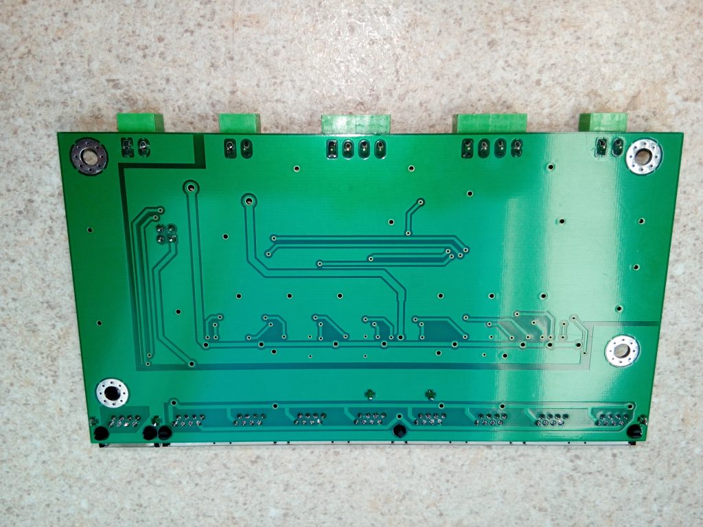
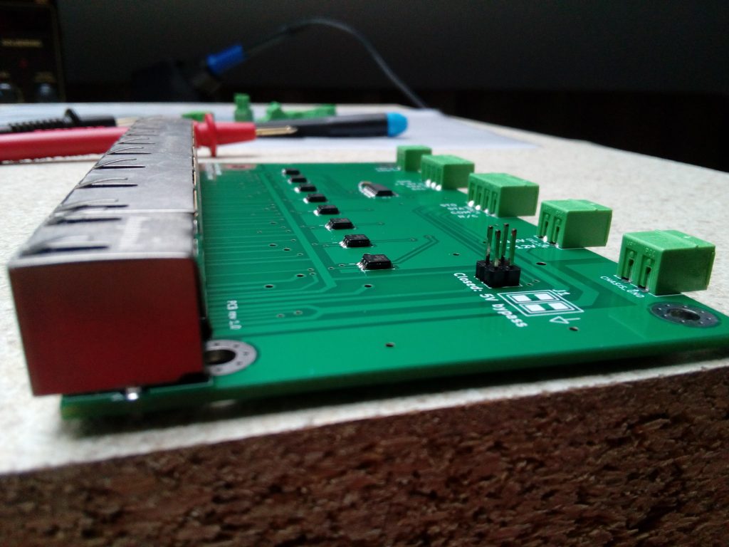
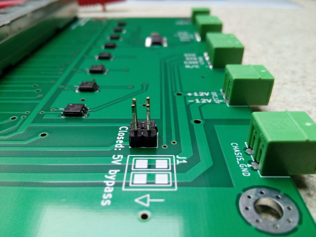
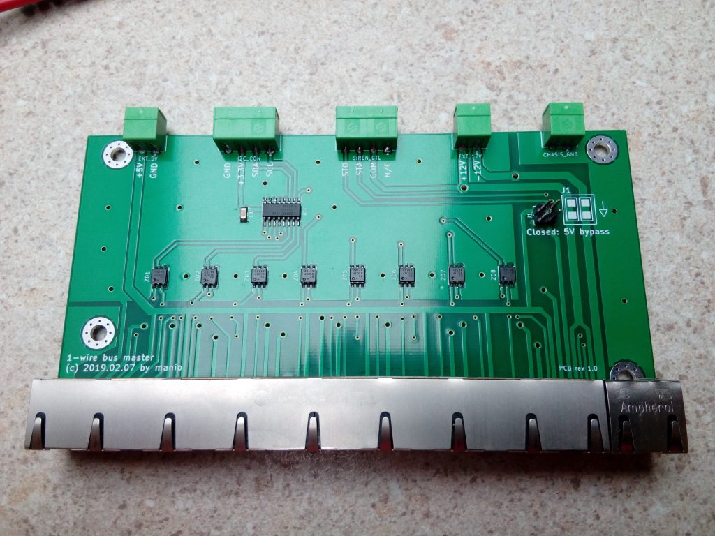
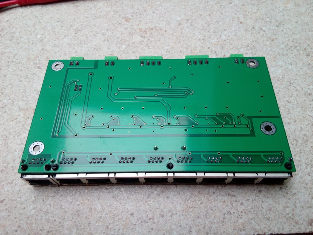
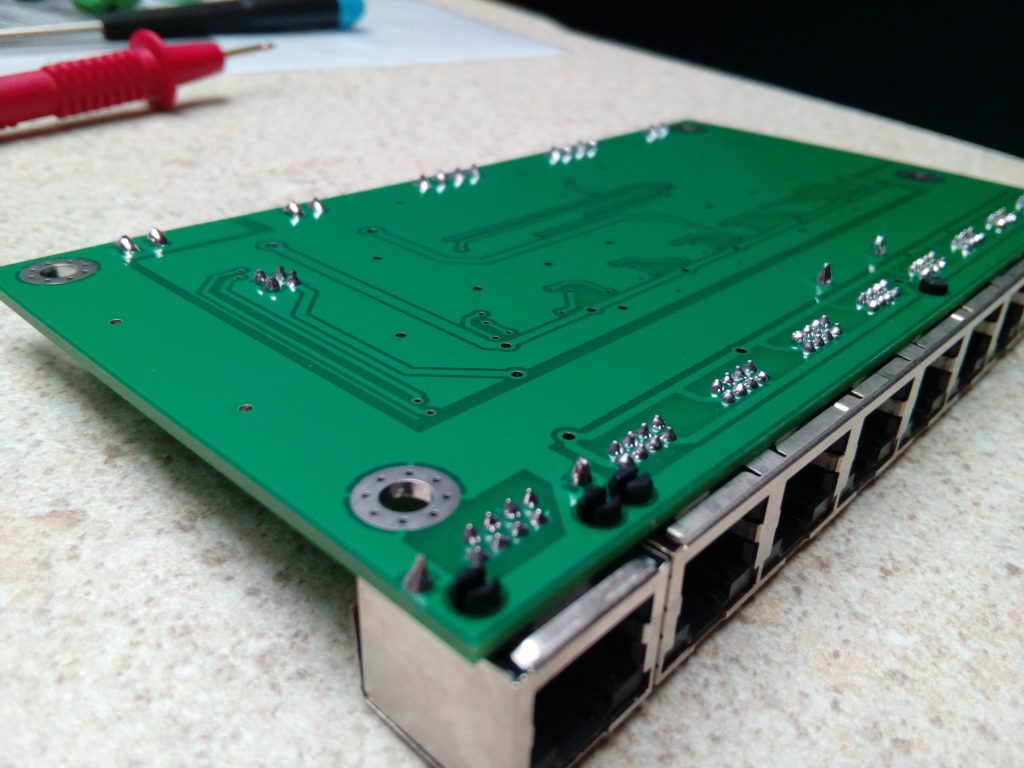
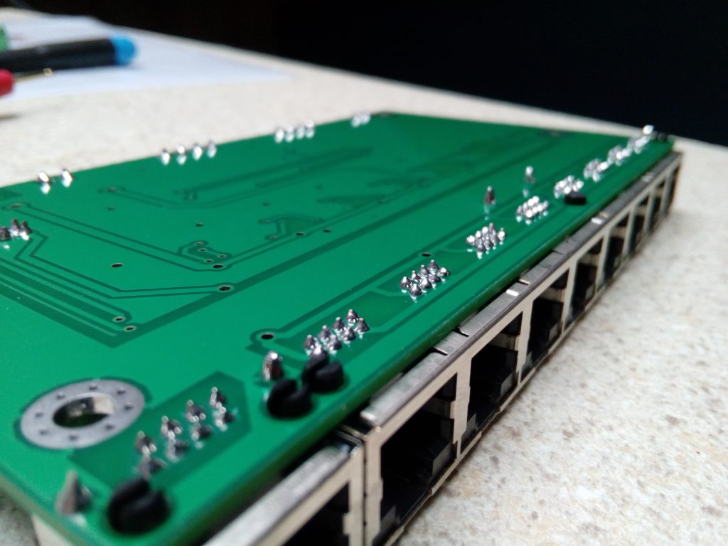
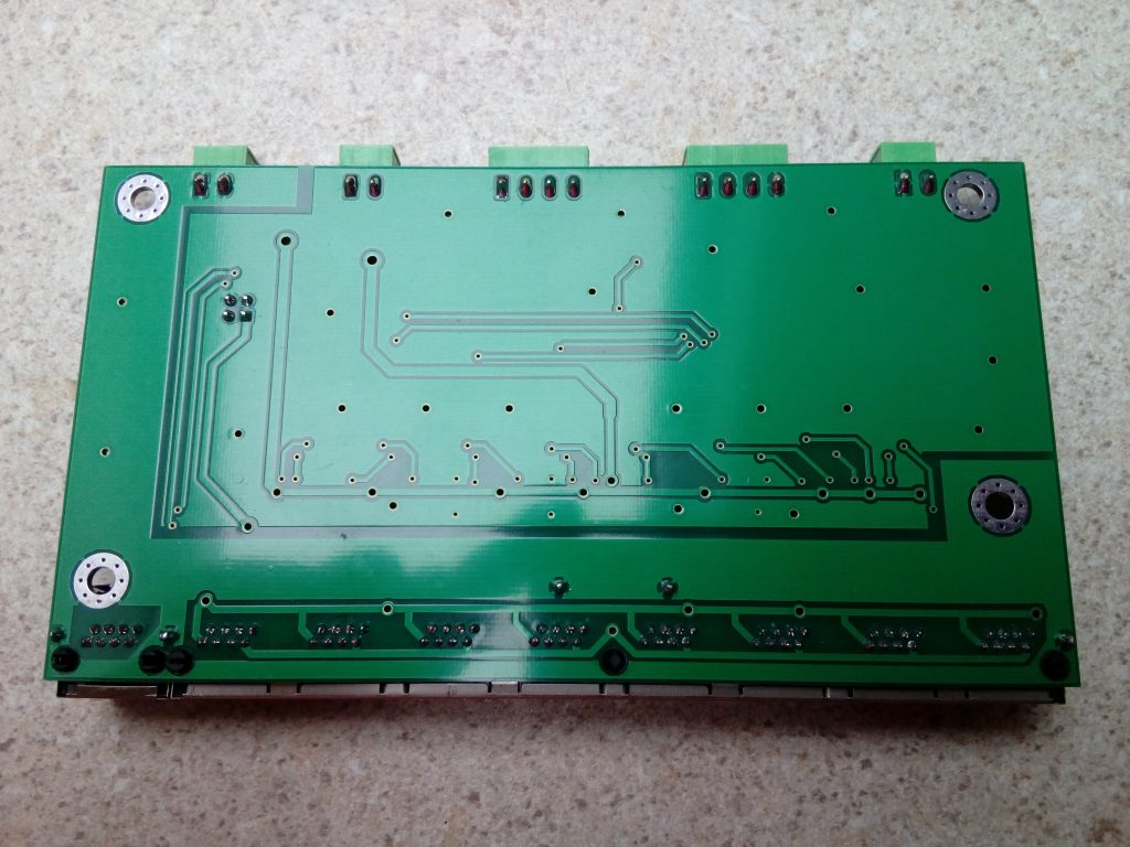
You’re probably curious how it all look like at the end. Here are the pictures: